
MQX.NeVa-M
Built for Fine Detail. Designed to Catch What Others Miss.
MQX.NeVa-M systems are purpose-built for inspecting small, complex, and high-precision components where even the tiniest defect can lead to major failure.
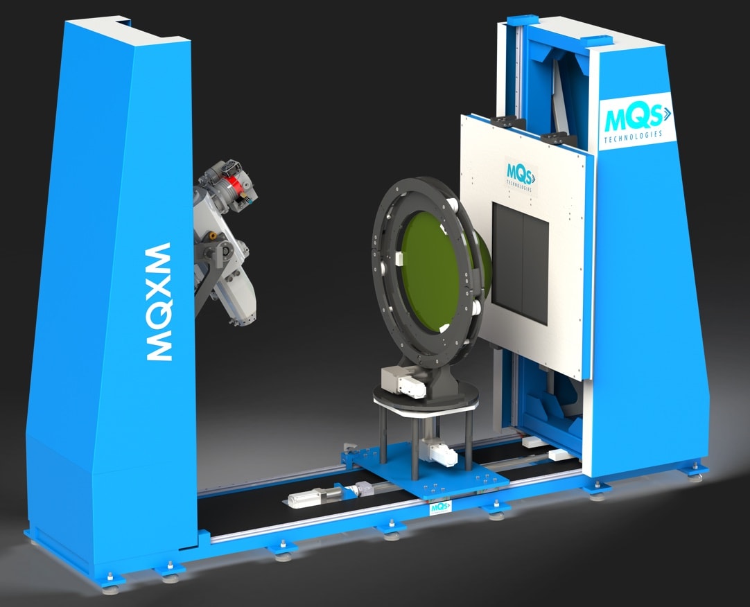
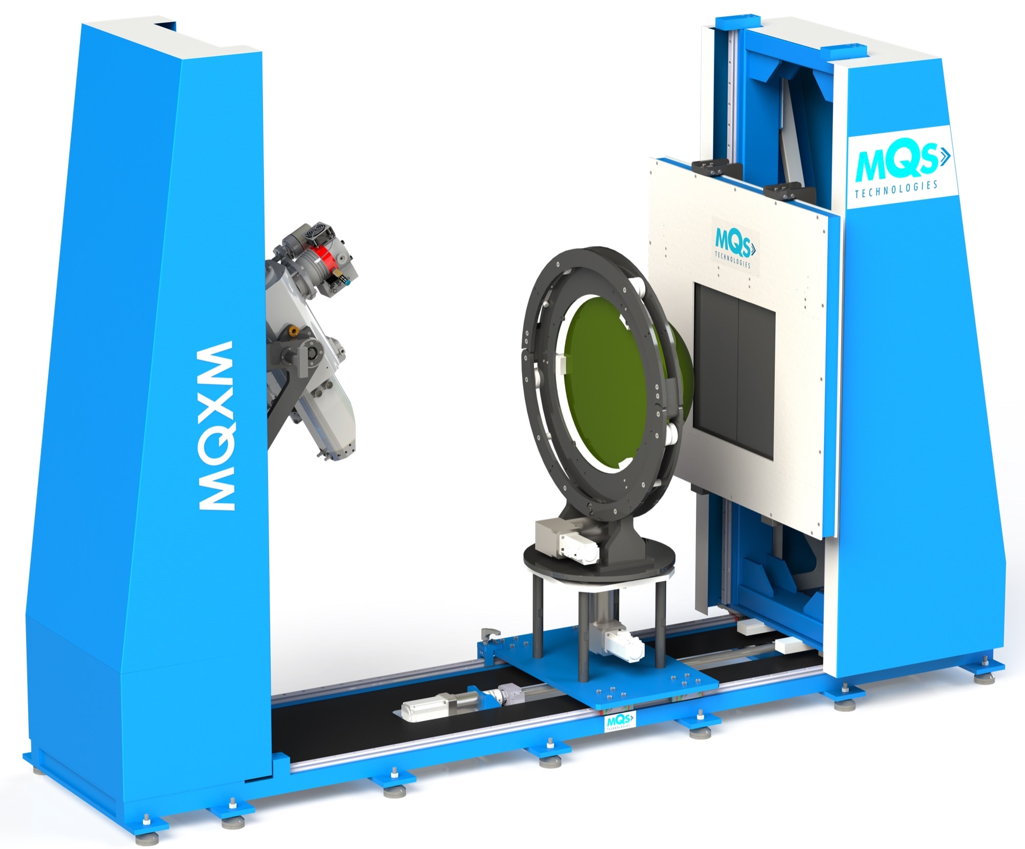
From PCB solder joints to aerospace composites, our systems deliver micron-scale imaging clarity with configurable tube technologies and modular architecture tailored to your application—supporting DR, CT, and panoramic inspection workflows.
Key Benefits
Ultra-High Resolution Imaging
Detect micro-cracks, porosities, inclusions, and bonding issues—down to 0.5 μm capability for precision-critical components.
One Platform for Mixed Materials
Wide operating range (160–300 kV) supports inspection from thin PCBs to dense aerospace alloys without switching platforms.
Faster Scans, Higher Throughput
High-power tube options and efficient cooling reduce scan time while preserving image quality—ideal for production and QC labs.
Flexible Inspection Modes
Support CT, DR, and panoramic imaging to handle different part geometries and failure modes without additional machines.
Future-Ready Analytics
Designed for integration with advanced analysis tools (e.g., VGStudio MAX, CT reconstruction, and AI-ready defect workflows) for smarter decisions.
Solution Highlights
Technical Data
Transmission Tube
- High resolution applications in electronic, automotive, aviation semiconductor industry, material science and space industries
- Down to 1 micron detail detectability and down to 0.2 micron high resolution target for computed tomography (CT) applications
- Single or double stage electron optics with condenser, centering and focusing coils
- Unsurpassed target power with target cooling and High Energy Target to reduce scanning time for computed tomography (CT) or Computed Laminography (CL) applications
Product line
Max. voltage
- Configuration
- Transmission · THE · 225 kV
- Min. voltage
- 20 kV
- Current
- 0.05 – 1 mA
- Max. power, target
- 10 W
- Max. power, emission
- 80 W
- JIMA resolution
- 2 µm
- Target material
- Beryllium / Tungsten
- Min. FOD
- 0.25 mm
- Opening angle
- ≈160°
- Tube weight
- ≈51 kg
Values from the MQMF brochure.
04
Flexible Inspection Modes
Support CT, DR, and panoramic imaging to handle different part geometries and failure modes without additional machines.
Digital Radiography
DR
Computed Tomography
CT
Rod Anode Tube