See hidden solder defects
Reveal BGA and QFN voids, cracks, bridging and head-in-pillow conditions that visual inspection can miss.
 Contact us
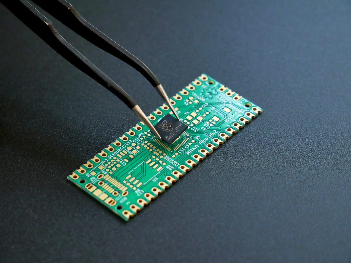
Electronics & semiconductors
Custom requirements. Engineered solution.
From SMT production to failure analysis, MQS X-ray and CT solutions reveal hidden solder, package and interconnect defects without damaging the assembly.
Talk to an ExpertIndustry overview
Electronics manufacturing is moving toward higher density, finer-pitch packages, multilayer assemblies and faster production cycles.
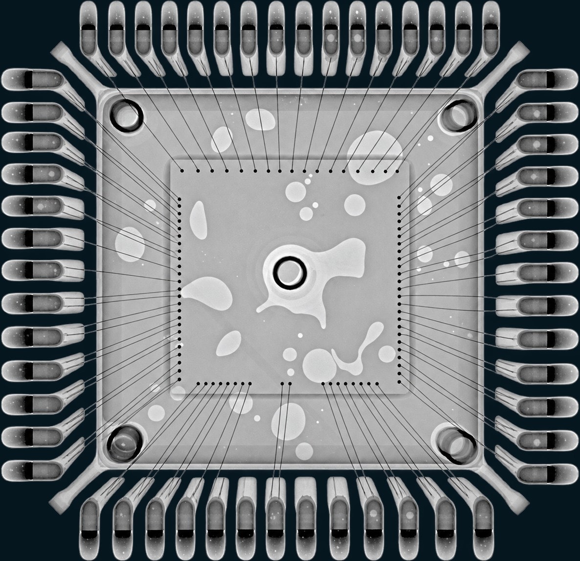
Defects such as voiding, bridging, head in pillow, lifted leads and insufficient solder fill can remain invisible to visual inspection and surface later as rework, yield loss or field failure. X-ray and CT reveal those internal connections without cutting the board.
What electronics QA teams need
Reveal BGA and QFN voids, cracks, bridging and head-in-pillow conditions that visual inspection can miss.
Separate layered boards and stacked features when a single 2D view leaves internal structures ambiguous.
Support fast, repeatable decisions without turning inspection into a production queue.
Build internal evidence before cutting a board or introducing additional rework risk.
Use measurement, pass/fail criteria and repeatable workflows to reduce operator subjectivity.
Count reel components accurately to prevent material mismatch and line stoppages.
Retain inspection images, measurements and reports for process analysis, customer review and audits.
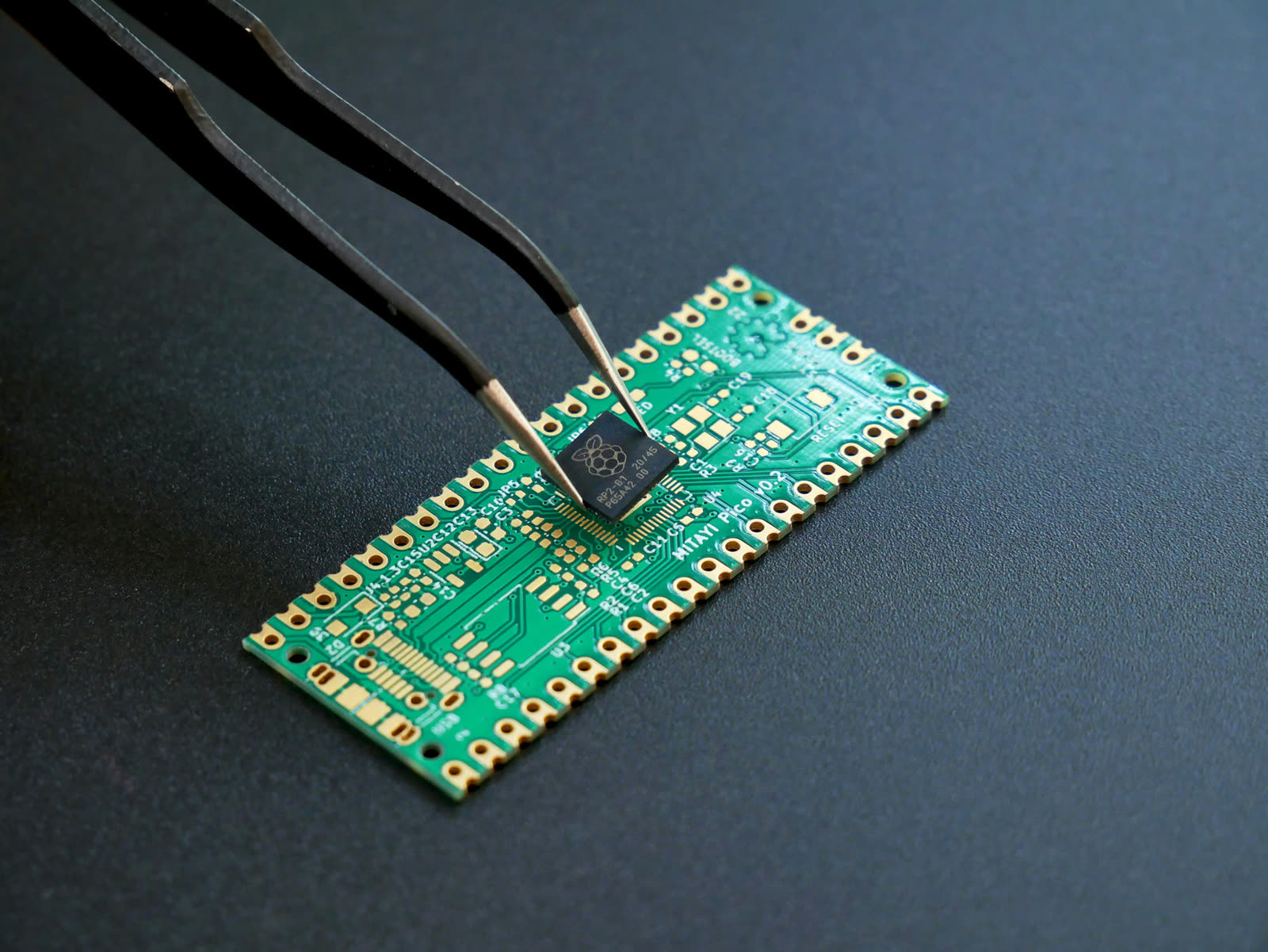
Application engineering
MQS starts with the board, package and defect target, then selects or configures the imaging chain, handling, automation and software needed to answer it.
PCB size, package type and density
Defect type, resolution and evidence
2D, 2.5D, CT or inline 3D
Handling, reporting and ERP / SPC
Standard platform or configured system
Built for production. Built for analysis.
Production screening, root-cause analysis, process control and material planning ask different questions.
Inspect solder joints quickly, with oblique views when straight 2D imaging is not enough.
Separate overlapping features and inspect internal layers without destructive sectioning.
Inspect within the production flow with automated defect analysis and board handling.
Apply measurement tools, pass/fail support and evidence-ready reporting.
Retain results and connect inspection data to production systems where configured.
Count components on reels quickly to support material planning and inventory accuracy.
Inspection concerns
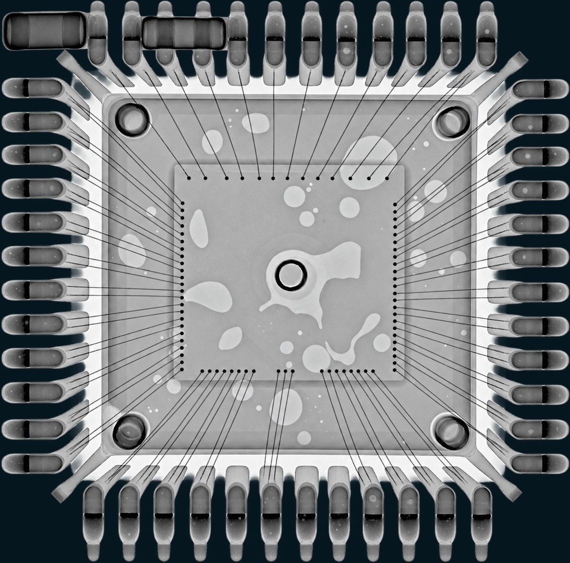
Internal void pattern, size and distribution within solder or die-attach regions.
Connection anomalies hidden beneath packages.
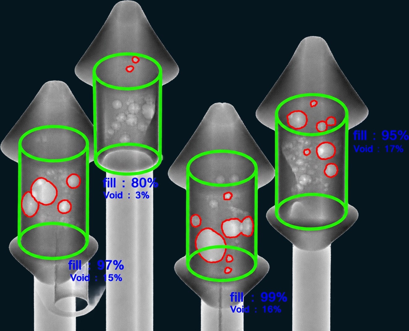
Barrel fill and void percentage for through-hole solder joints.
Internal package features, bond-wire condition and die-attach voiding.
CT slices that separate stacked features and reveal the true internal structure.
Internal discontinuities that may not be visible from the surface.
X-ray-based component counting for reel inventory and planning.
MQS electronics portfolio
Move from fast screening to CT analysis, inline automation and inventory control using the platform matched to the question.
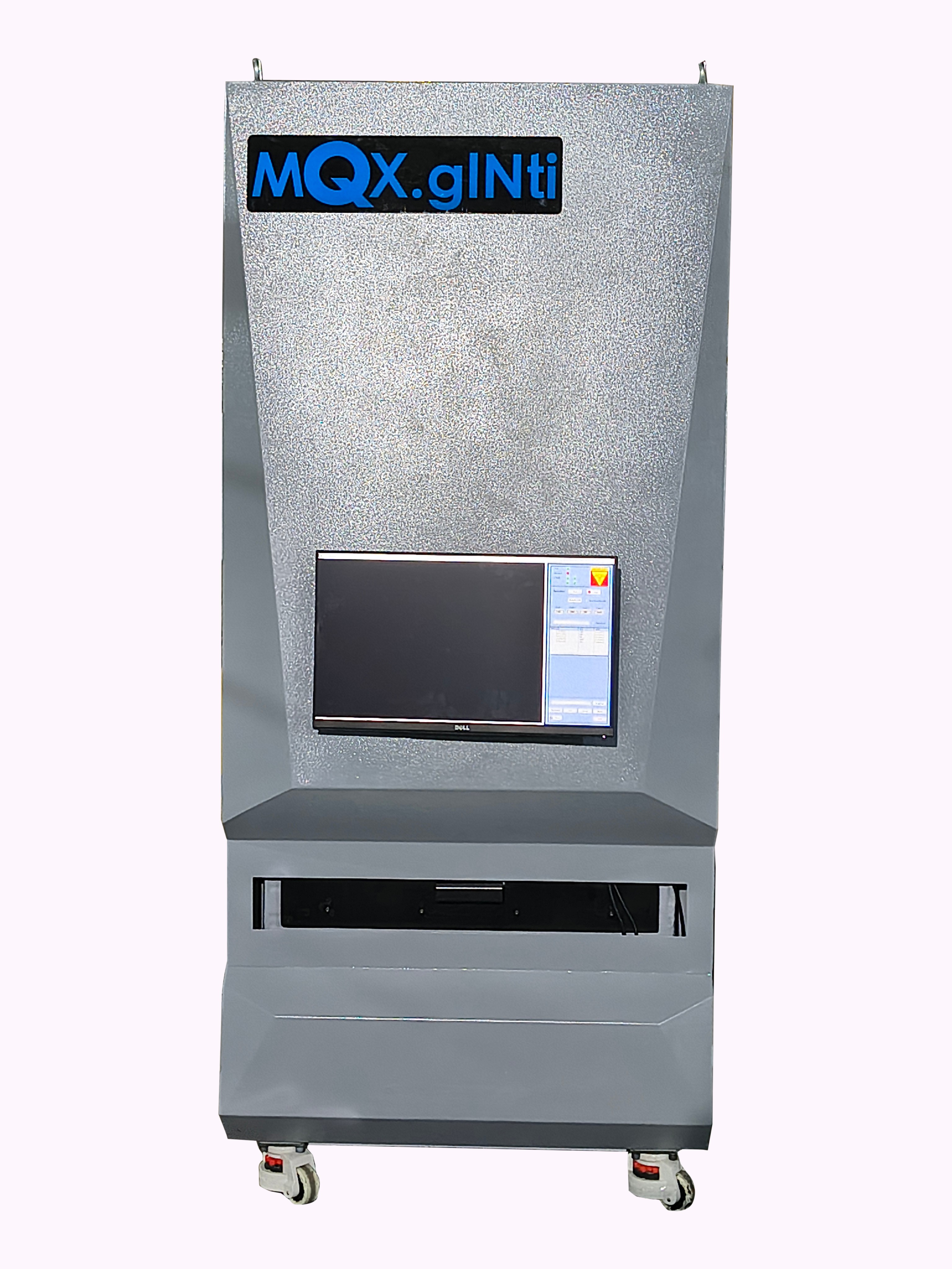
AI component counting
Fast, accurate SMT reel counts that support inventory planning and reduce material-related line stoppages.
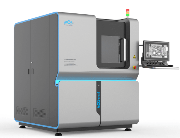
2.5D PCB X-ray inspection
Fast inspection of BGA, QFN, PTH and common SMT defect conditions without damaging the assembly.
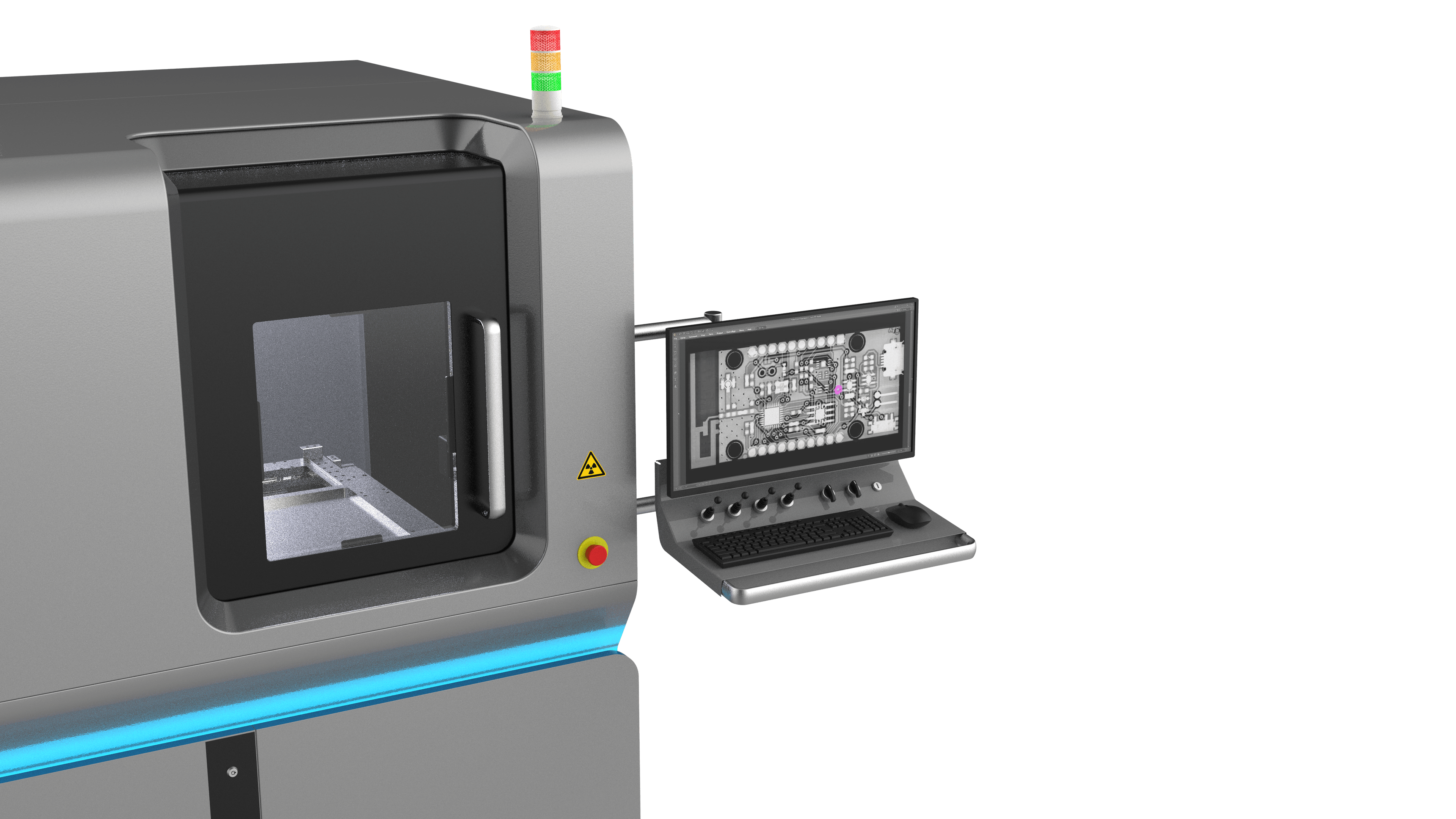
2D screening with 3D CT
Layer-by-layer analysis, root-cause confirmation and traceable reporting when overlap creates ambiguity.
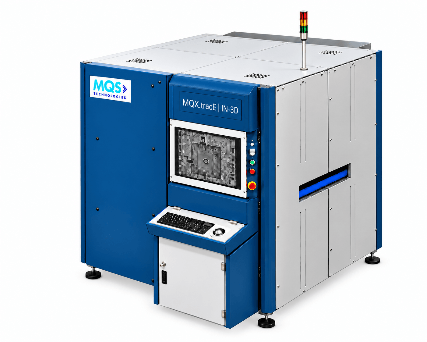
Inline 2D / 2.5D / 3D
Automated inspection and board handling inside the production flow rather than at an offline station.
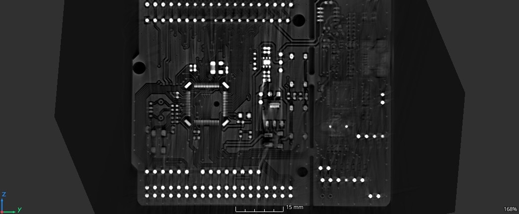
Fine-detail X-ray / CT
Finer internal detail for package analysis, R&D and failure investigation beyond routine board screening.
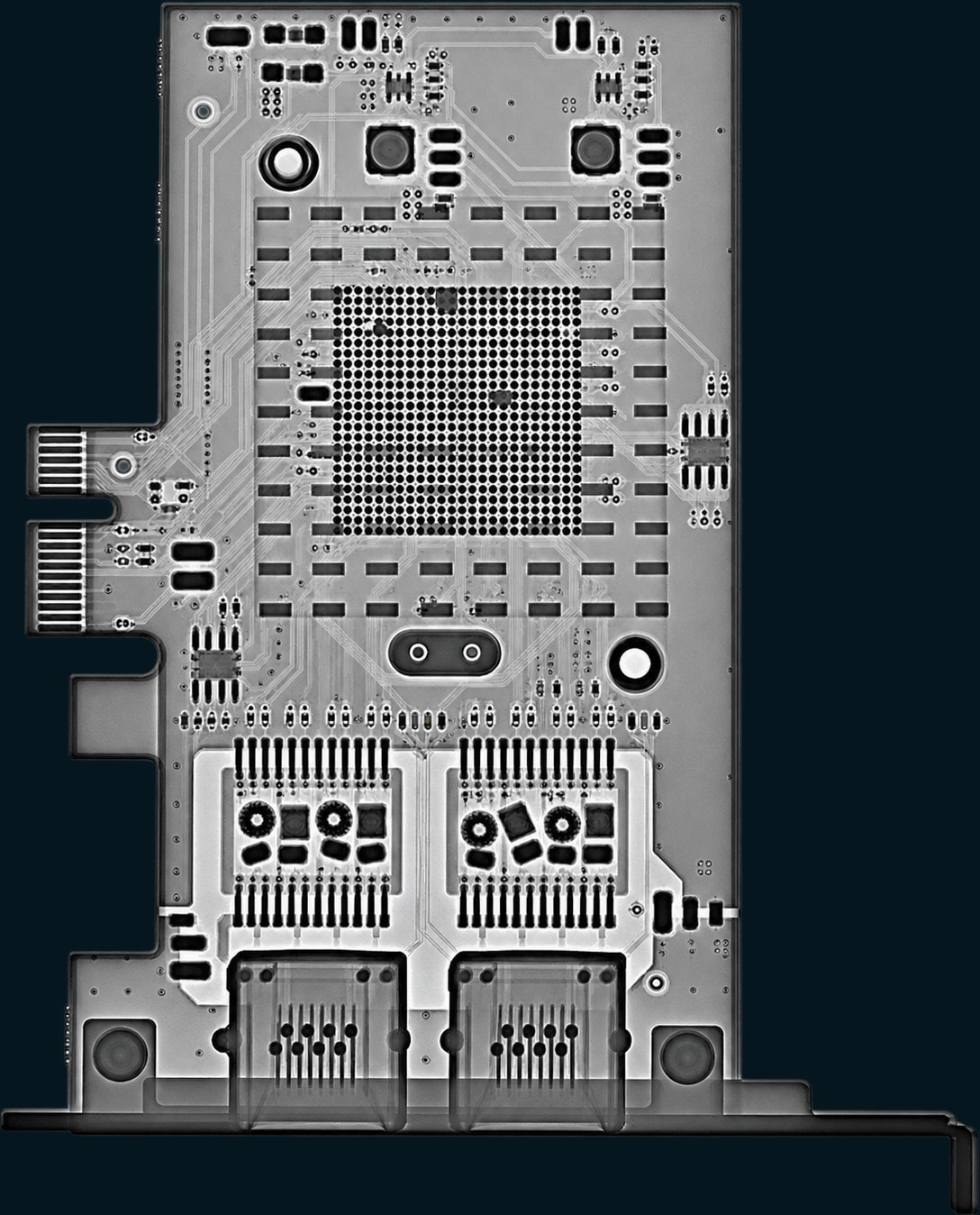
Inspection evidence
Indigenous engineering
Standard where it works. Custom where it matters.
MQS starts with a proven inspection platform, then adapts imaging, handling, automation, analysis, reporting and integration where the process requires it. Design ownership and long-term engineering support let the system evolve with the production line.
Resources
Move directly from the inspection question to the relevant platform information.
Bring us the board. We’ll engineer the inspection.
Share the package, defect target, throughput requirement and traceability need.
Share your part, material and defect type — our engineers will recommend the right MQS system.